Silicon Photonics vs. Copper: Solving the 800G Data Center Bottleneck
Advertisements

Silicon photonics is emerging as a critical solution for addressing the 800G data center bottleneck, offering superior bandwidth, energy efficiency, and reach compared to traditional copper interconnects.
The relentless demand for faster data processing and transmission in modern data centers has brought the industry to a critical juncture. As we push towards 800G and beyond, the limitations of traditional copper interconnects are becoming increasingly apparent, creating a significant bottleneck. This article delves into how silicon photonics data centers are not just an alternative but a necessary evolution to meet these escalating demands.
The looming 800G data center bottleneck
Data centers are the backbone of our digital world, powering everything from cloud computing to artificial intelligence. As the volume of data generated and processed continues to explode, the demand for higher bandwidth and lower latency within these facilities is insatiable. The transition from 400G to 800G Ethernet is already underway, and it presents formidable challenges for the underlying interconnect infrastructure.
Traditional copper cables, while cost-effective and reliable for shorter distances and lower speeds, are reaching their physical limits. At 800G and beyond, copper suffers from significant signal degradation, increased power consumption, and bulkiness, making it impractical for the high-density, high-speed environments of modern data centers. This bottleneck threatens to impede the progress of critical technologies and applications.
Challenges with traditional copper at 800G
As data rates climb, several factors conspire to make copper less viable:
- Signal Attenuation: Higher frequencies lead to greater signal loss over distance, requiring more repeaters and increasing complexity.
- Crosstalk: Electromagnetic interference between adjacent wires becomes more pronounced, corrupting data signals.
- Power Consumption: Driving high-speed signals over copper requires significant power, leading to higher operational costs and heat generation.
- Physical Bulk: Thick copper cables consume valuable rack space and impede airflow, complicating cooling.
Addressing these challenges effectively requires a fundamental shift in how data is transmitted within the data center. The sheer volume of data, coupled with the need for ultra-low latency, necessitates a solution that can handle higher bandwidth with greater efficiency and less physical footprint. The limitations of copper are not merely an engineering hurdle but a foundational barrier to future data center scalability.
In conclusion, the move to 800G and beyond exposes the inherent limitations of copper interconnects. The need for a more robust, efficient, and scalable solution is paramount, pushing the industry to explore and adopt alternative technologies that can meet the rigorous demands of next-generation data centers.
Understanding silicon photonics: A technological paradigm shift
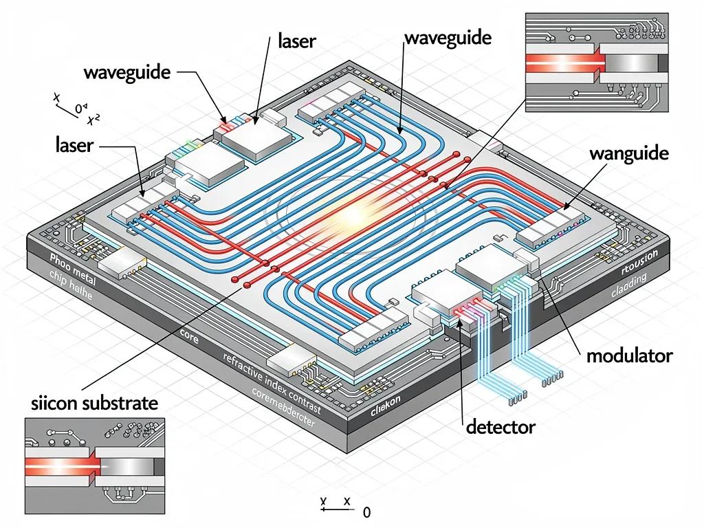
Silicon photonics represents a revolutionary approach to data transmission, integrating optical components onto a silicon chip. This technology leverages the speed of light to move data, offering a dramatic improvement over electrical signals carried by copper. By fabricating optical waveguides, modulators, and detectors directly onto silicon wafers using standard CMOS manufacturing processes, silicon photonics enables high-volume, low-cost production of complex optical circuits.
The core idea behind silicon photonics is to replace bulky, discrete optical components with miniaturized, integrated versions. This integration not only reduces size and cost but also significantly improves performance. Light, traveling through optical fibers, experiences far less attenuation and interference than electrical signals, allowing for much greater distances and higher data rates.
Key components of a silicon photonics chip
A typical silicon photonics chip integrates several critical elements:
- Waveguides: Tiny channels that guide light across the chip, acting as optical wires.
- Modulators: Devices that encode electrical data onto light signals.
- Detectors: Components that convert incoming light signals back into electrical data.
- Lasers: While sometimes integrated, external lasers are often coupled to the chip to provide the light source.
This integration capability is what makes silicon photonics so powerful. It allows for the creation of compact, energy-efficient transceivers that can handle massive amounts of data. The ability to leverage existing silicon manufacturing infrastructure also provides a clear path to scaling production and reducing costs, making it an economically attractive solution for widespread adoption in data centers.
In essence, silicon photonics is not just about using light instead of electricity; it's about miniaturizing and integrating the entire optical communication system onto a single, mass-producible chip. This fundamental shift promises to unlock unprecedented levels of performance and efficiency for data transmission, laying the groundwork for the next generation of high-speed networks.
Advantages of silicon photonics over copper interconnects
The transition to silicon photonics data centers brings a myriad of advantages that directly address the limitations of traditional copper. These benefits extend across performance, energy efficiency, physical footprint, and scalability, making silicon photonics a compelling choice for future data infrastructure.
One of the most significant advantages is the sheer bandwidth capability. Optical fibers can carry far more data per second than copper wires, enabling much higher data rates over longer distances without signal degradation. This is crucial for 800G and beyond, where copper simply cannot keep up without extensive and costly signal conditioning.
Performance and efficiency gains
- Higher Bandwidth: Light signals can transmit terabits per second, far exceeding copper's capabilities.
- Lower Latency: Light travels faster and with fewer impedance issues than electrons, reducing transmission delays.
- Reduced Power Consumption: Optical transceivers consume significantly less power per bit than copper-based electrical transceivers, leading to substantial energy savings.
- Longer Reach: Optical signals maintain integrity over much greater distances, simplifying data center architecture and reducing the need for signal repeaters.
Beyond raw performance, the energy efficiency of silicon photonics is a critical factor. Data centers are enormous consumers of electricity, and reducing power draw directly translates to lower operational costs and a smaller carbon footprint. The ability to transmit more data with less energy is a game-changer for sustainability and economic viability.
Furthermore, the physical characteristics of optical fibers are inherently superior. They are thinner, lighter, and immune to electromagnetic interference, which is a constant challenge with copper. This allows for higher density cabling, better airflow, and easier management within crowded data center racks, directly impacting cooling efficiency and maintenance.
In summary, silicon photonics provides a comprehensive solution that not only overcomes the technical limitations of copper at high speeds but also delivers significant operational and environmental benefits. It’s a technology that aligns perfectly with the evolving needs of modern, high-performance data centers.
Integrating silicon photonics into existing data center infrastructure
While the benefits of silicon photonics are clear, the integration into existing data center infrastructure presents its own set of considerations. Data centers represent massive investments, and a complete overhaul is often impractical. The key lies in a phased approach, leveraging the modularity and compatibility of silicon photonics solutions to gradually upgrade and enhance capabilities.
Modern silicon photonics transceivers are designed to fit into standard form factors, such as QSFP-DD and OSFP, which are already prevalent in data centers. This allows for a relatively straightforward swap-out of copper-based transceivers with optical ones, enabling a seamless upgrade path without requiring a complete redesign of network equipment or server racks.
Deployment strategies and considerations
Successful integration often involves:
- Phased Upgrades: Prioritizing upgrades in high-bandwidth areas, such as spine-leaf architectures and inter-rack connections, where the bottleneck is most acute.
- Hybrid Approaches: Utilizing copper for shorter, lower-speed links (e.g., within a server rack) and silicon photonics for longer, higher-speed connections (e.g., between racks or across the data center).
- Standardization: Adhering to industry standards for optical interfaces and connectors to ensure interoperability and avoid vendor lock-in.
Another crucial aspect is the management of optical fiber cabling. While optical fibers are superior in performance, they require different handling and maintenance procedures compared to copper. Training for technicians and the implementation of appropriate fiber management systems are essential to ensure reliability and minimize downtime.
The cost effectiveness of silicon photonics is also improving rapidly. As manufacturing processes mature and economies of scale are achieved, the price per bit transmitted continues to decrease, making it a more attractive option for large-scale deployments. Initial investment costs are often offset by long-term operational savings in power and cooling.
Ultimately, integrating silicon photonics is not about replacing everything overnight, but rather strategically deploying it where it delivers the most impact. This measured approach allows data center operators to harness the power of optical communication while managing costs and minimizing disruption to existing operations.
The economic and environmental impact of optical interconnects
The shift towards optical interconnects, particularly silicon photonics data centers, carries significant economic and environmental implications. Beyond just technical performance, these factors are increasingly driving adoption as organizations seek to optimize their bottom line and meet sustainability goals.
Economically, the initial investment in optical transceivers and fiber infrastructure can be higher than traditional copper. However, this upfront cost is often quickly recouped through substantial operational savings. The most significant saving comes from reduced power consumption. Less power for data transmission means lower electricity bills and, critically, less heat generation, which in turn reduces cooling costs—a major expense for data centers.
Long-term cost savings and sustainability
- Lower Energy Bills: Reduced power consumption for data transmission and cooling leads to significant operational cost savings over the lifespan of the data center.
- Reduced Infrastructure Complexity: Longer reach of optical signals can simplify network architecture, potentially reducing the need for intermediate switches or repeaters.
- Smaller Carbon Footprint: Lower energy consumption directly translates to reduced greenhouse gas emissions, helping data centers meet increasingly stringent environmental regulations and corporate sustainability targets.
- Increased Rack Density: Thinner optical cables allow for more equipment in less space, optimizing real estate utilization within the data center.
Environmentally, the impact is profound. Data centers are notorious energy hogs, and any technology that can significantly reduce their power footprint is a step forward for sustainability. Silicon photonics contributes to a greener data center by making data transmission inherently more energy-efficient and by alleviating the cooling burden.
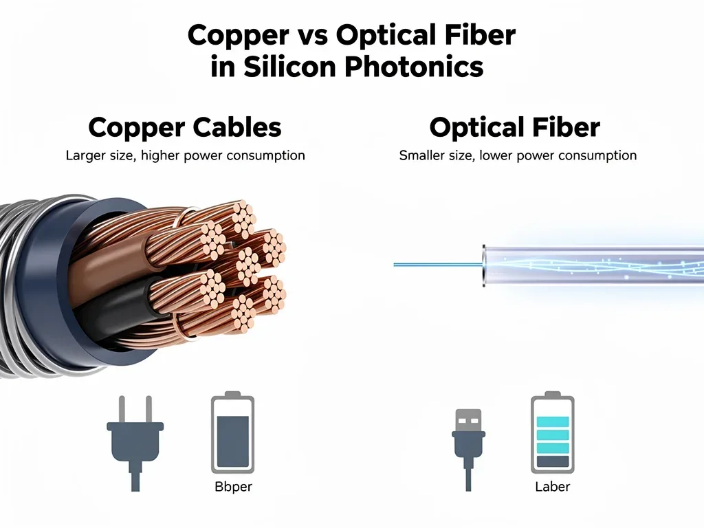
Moreover, the reduced physical volume of optical cabling compared to copper bundles can lead to less material usage and easier recycling at end-of-life, though the environmental impact of chip manufacturing itself remains an area of ongoing research and improvement. The ability to pack more bandwidth into a smaller space also means that data centers can grow without necessarily expanding their physical footprint as rapidly.
In conclusion, while the upfront costs might seem higher, the long-term economic benefits and environmental advantages of silicon photonics make it a strategically sound investment. It provides a pathway to more sustainable, cost-effective, and high-performing data center operations.
Future outlook: Beyond 800G and the evolution of silicon photonics
The journey for silicon photonics doesn't end at 800G; it's merely a stepping stone. As demand for data continues its exponential growth, data centers are already looking towards 1.6T and even 3.2T Ethernet. Silicon photonics is uniquely positioned to scale to these future requirements, offering a clear roadmap for continued bandwidth expansion.
Innovations in silicon photonics are rapidly advancing. Researchers are exploring higher levels of integration, including the integration of lasers directly onto the silicon chip, which would further reduce cost, power consumption, and manufacturing complexity. This move towards fully integrated silicon photonic systems will unlock even greater performance potential.
Emerging trends and advancements
- Co-packaged Optics (CPO): Integrating optical transceivers directly into the same package as high-bandwidth switches and processors, dramatically shortening electrical traces and reducing power.
- Photonic AI Accelerators: Leveraging the speed of light for ultra-fast matrix multiplication and other computations directly on-chip, potentially revolutionizing AI processing.
- Quantum Computing Interconnects: Silicon photonics is being explored as a viable platform for interconnecting quantum processors, given its low loss and high bandwidth.
The convergence of photonics and electronics on a single platform also opens up possibilities for novel architectures. Imagine processors communicating with memory and other processors entirely with light, eliminating the electrical bottleneck at every level. This vision, while still in its early stages, highlights the transformative potential of silicon photonics.
Furthermore, the manufacturing ecosystem for silicon photonics is maturing, with more foundries offering fabrication services and a growing talent pool. This industrialization will drive down costs and accelerate innovation, making these advanced optical solutions more accessible to a wider range of applications beyond just data centers, such as telecommunications and automotive LiDAR.
In summary, the future of silicon photonics is bright and extends far beyond merely solving today's 800G bottleneck. It represents a fundamental shift in how we design and build high-performance computing and communication systems, promising a future of unprecedented speed, efficiency, and integration.
Challenges and considerations for widespread adoption
While the advantages of silicon photonics are compelling, its widespread adoption isn't without challenges. Overcoming these hurdles is crucial for realizing the full potential of this transformative technology in silicon photonics data centers and beyond.
One significant challenge is the expertise gap. Designing, deploying, and maintaining optical networks requires a different skill set than traditional electrical networks. Training and upskilling the workforce will be essential to ensure smooth transitions and effective operations. This includes everything from fiber handling best practices to troubleshooting complex optical circuits.
Overcoming adoption hurdles
- Cost of Transition: While operational costs are lower, the initial investment in new optical equipment can be substantial for some organizations.
- Interoperability: Ensuring seamless communication between different vendors' optical components and existing network infrastructure requires robust standardization efforts.
- Reliability and Durability: As a relatively newer technology for mass deployment, long-term reliability and durability under various data center conditions need continuous validation and improvement.
- Thermal Management: Although more energy-efficient, the high integration density of silicon photonics chips can still pose thermal management challenges that need careful engineering.
Another consideration is the supply chain. As demand for silicon photonics devices grows, ensuring a robust and resilient supply chain for components, from specialized wafers to packaging materials, will be critical. Diversification of suppliers and manufacturing locations can mitigate potential risks.
The industry is actively working to address these challenges. Standardization bodies are developing new specifications, manufacturers are refining their processes to improve reliability and reduce costs, and educational institutions are incorporating photonics into their curricula. Collaborative efforts across the ecosystem, involving chip designers, equipment manufacturers, and data center operators, are key to accelerating adoption.
In conclusion, while silicon photonics offers a clear path forward for high-speed data centers, a strategic and collaborative approach is needed to navigate the challenges of widespread adoption. Addressing these issues systematically will pave the way for a future dominated by light-speed communication.
| Key Point | Brief Description |
|---|---|
| 800G Bottleneck | Traditional copper interconnects struggle with signal integrity, power, and bulk at 800G and higher data rates. |
| Silicon Photonics | Integrates optical components onto a silicon chip, using light for data transmission, offering superior performance. |
| Key Advantages | Higher bandwidth, lower latency, reduced power consumption, longer reach, and smaller physical footprint. |
| Future Outlook | Scalable to 1.6T and beyond, with advancements like co-packaged optics and photonic AI accelerators. |
Frequently asked questions about silicon photonics
What is silicon photonics and how does it differ from traditional electronics?▼Silicon photonics integrates optical components onto a silicon chip, transmitting data using light instead of electricity. Unlike traditional electronics that use electrons, photonics leverages photons, offering higher speeds, lower power consumption, and greater bandwidth over longer distances, crucial for modern data centers.
Why are copper interconnects becoming a bottleneck for 800G data centers?▼At 800G speeds, copper interconnects face severe limitations including significant signal attenuation, increased crosstalk, high power consumption, and physical bulk. These issues degrade data integrity, increase operational costs, and hinder the high-density requirements of advanced data centers, creating a performance bottleneck.
What are the main advantages of using silicon photonics in data centers?▼Silicon photonics offers several key advantages: higher bandwidth capacity, lower power consumption per bit, reduced latency, longer transmission reach, and a smaller physical footprint for cabling. These benefits lead to more efficient, scalable, and environmentally friendly data center operations.
Is silicon photonics ready for widespread adoption in data centers?▼Yes, silicon photonics is increasingly ready. It's being integrated into standard form factors, allowing for phased upgrades. While challenges like cost and expertise gaps remain, ongoing innovations, standardization efforts, and a maturing supply chain are accelerating its widespread deployment in high-speed data centers.
What is the future potential of silicon photonics beyond 800G?▼Beyond 800G, silicon photonics is critical for scaling to 1.6T and 3.2T Ethernet. Future advancements include co-packaged optics, photonic AI accelerators, and potential applications in quantum computing interconnects, promising even greater integration, speed, and energy efficiency for future computing architectures.
Conclusion
The journey from traditional copper interconnects to advanced silicon photonics is not merely an incremental upgrade but a fundamental transformation driven by the escalating demands of modern data centers. As we confront the 800G bottleneck, silicon photonics emerges as the unequivocal solution, offering unparalleled bandwidth, superior energy efficiency, and a dramatically reduced physical footprint. This technology is not just addressing current challenges but is also laying the groundwork for the next generations of data processing and communication, promising a future where data moves at the speed of light, with greater sustainability and scalability. The continued innovation and strategic adoption of silicon photonics will be pivotal in shaping the future of our digital infrastructure.
